2025
Boddison-Chouinard, Justin; Korkusinski, Marek; Bogan, Alex; Barrios, Pedro; Waldron, Philip; Watanabe, Kenji; Taniguchi, Takashi; Pawłowski, Jarosław; Miravet, Daniel; Hawrylak, Pawel; Luican-Mayer, Adina; Gaudreau, Louis
Valley-spin polarization at zero magnetic field induced by strong hole-hole interactions in monolayer WSe2 Journal Article
In: Science Advances, vol. 11, no. 19, pp. eadu4696, 2025.
@article{doi:10.1126/sciadv.adu4696,
title = {Valley-spin polarization at zero magnetic field induced by strong hole-hole interactions in monolayer WSe_{2}},
author = {Justin Boddison-Chouinard and Marek Korkusinski and Alex Bogan and Pedro Barrios and Philip Waldron and Kenji Watanabe and Takashi Taniguchi and Jarosław Pawłowski and Daniel Miravet and Pawel Hawrylak and Adina Luican-Mayer and Louis Gaudreau},
url = {https://www.science.org/doi/abs/10.1126/sciadv.adu4696},
doi = {10.1126/sciadv.adu4696},
year = {2025},
date = {2025-01-01},
journal = {Science Advances},
volume = {11},
number = {19},
pages = {eadu4696},
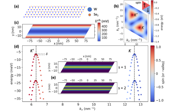
abstract = {Monolayer transition metal dichalcogenides have emerged as prominent candidates to explore the complex interplay between spin and valley degrees of freedom. Their strong spin-orbit interaction and broken inversion symmetry lead to the spin-valley locking effect, in which carriers occupying the K and K′ valleys of the reciprocal space must have opposite spins. This effect is particularly strong for holes due to a larger spin-orbit gap in the valence band. By reducing the dimensionality of a monolayer of WSe2 to 1D via electrostatic confinement, we demonstrate that spin-valley locking and strong hole-hole interactions lead to a ferromagnetic state where hole transport is spin-valley polarized, even without an applied magnetic field. A massive Dirac fermion model in the Hartree-Fock approximation reveals that many-body hole-exchange interactions lead to this polarized ground-state. This observation opens the possibility of implementing a robust and stable valley-polarized system, essential in valleytronic applications. Strong hole-hole interactions and spin-orbit coupling lead to a valley-polarized state in 1D confined monolayer WSe2.},
keywords = {},
pubstate = {published},
tppubtype = {article}
}
2024
Pawłowski, Jarosław; Miravet, Daniel; Bieniek, Maciej; Korkusinski, Marek; Boddison-Chouinard, Justin; Gaudreau, Louis; Luican-Mayer, Adina; Hawrylak, Pawel
Interacting holes in a gated WSe2 quantum channel: valley correlations and zigzag Wigner crystal Journal Article
In: arXiv e-prints, 2024.
@article{arXiv:2406.08655,

title = {Interacting holes in a gated WSe2 quantum channel: valley correlations and zigzag Wigner crystal},

author = {Jarosław Pawłowski and Daniel Miravet and Maciej Bieniek and Marek Korkusinski and Justin Boddison-Chouinard and Louis Gaudreau and Adina Luican-Mayer and Pawel Hawrylak},

url = {https://arxiv.org/abs/2406.08655#},

doi = {2406.08655},

year  = {2024},

date = {2024-06-12},

urldate = {2024-06-12},

journal = {arXiv e-prints},

abstract = {We present a theory of interacting valence holes in a gate-defined one-dimensional quantum channel in a single layer of a transition metal dichalcogenide material WSe2. Based on a microscopic atomistic tight-binding model and Hartree-Fock and exact configuration-interaction tools we demonstrate the possibility of symmetry-broken valley polarized states for strongly interacting holes. The interplay between interactions, perpendicular magnetic field, and the lateral confinement asymmetry together with the strong Rashba spin-orbit coupling present in WSe2 material is analyzed, and its impact on valley polarization is discussed. For weaker interactions, an investigation of the pair correlation function reveals a valley-antiferromagnetic phase. For low hole densities, a formation of a zigzag Wigner crystal phase is predicted. The impact of various hole liquid phases on transport in a high mobility quasi-one dimensional channel is discussed. },

keywords = {},

pubstate = {published},

tppubtype = {article}

}
2023
Molino, Laurent; Aggarwal, Leena; Maity, Indrajit; Plumadore, Ryan; Lischner, Johannes; Luican-Mayer, Adina
Influence of Atomic Relaxations on the Moiré Flat Band Wave Functions in Antiparallel Twisted Bilayer WS2 Journal Article
In: Nano Lett., vol. 23, no. 24, pp. 11778–11784, 2023, ISSN: 1530-6992.
@article{Molino2023,

title = {Influence of Atomic Relaxations on the Moiré Flat Band Wave Functions in Antiparallel Twisted Bilayer WS_{2}},

author = {Laurent Molino and Leena Aggarwal and Indrajit Maity and Ryan Plumadore and Johannes Lischner and Adina Luican-Mayer},

doi = {10.1021/acs.nanolett.3c03735},

issn = {1530-6992},

year  = {2023},

date = {2023-12-27},

urldate = {2023-12-27},

journal = {Nano Lett.},

volume = {23},

number = {24},

pages = {11778--11784},

publisher = {American Chemical Society (ACS)},

keywords = {},

pubstate = {published},

tppubtype = {article}

}
Jiménez-Galán, Álvaro; Bossaer, Chandler; Ernotte, Guilmot; Parks, Andrew M.; Silva, Rui E. F.; Villeneuve, David M.; Staudte, André; Brabec, Thomas; Luican-Mayer, Adina; Vampa, Giulio
Orbital perspective on high-harmonic generation from solids Journal Article
In: Nat Commun, vol. 14, no. 1, 2023, ISSN: 2041-1723.
@article{Jiménez-Galán2023b,

title = {Orbital perspective on high-harmonic generation from solids},

author = {Álvaro Jiménez-Galán and Chandler Bossaer and Guilmot Ernotte and Andrew M. Parks and Rui E. F. Silva and David M. Villeneuve and André Staudte and Thomas Brabec and Adina Luican-Mayer and Giulio Vampa},

doi = {10.1038/s41467-023-44041-0},

issn = {2041-1723},

year  = {2023},

date = {2023-12-18},

urldate = {2023-12-18},

journal = {Nat Commun},

volume = {14},

number = {1},

publisher = {Springer Science and Business Media LLC},

abstract = {<jats:title>Abstract</jats:title><jats:p>High-harmonic generation in solids allows probing and controlling electron dynamics in crystals on few femtosecond timescales, paving the way to lightwave electronics. In the spatial domain, recent advances in the real-space interpretation of high-harmonic emission in solids allows imaging the field-free, static, potential of the valence electrons with picometer resolution. The combination of such extreme spatial and temporal resolutions to measure and control strong-field dynamics in solids at the atomic scale is poised to unlock a new frontier of lightwave electronics. Here, we report a strong intensity-dependent anisotropy in the high-harmonic generation from ReS<jats:sub>2</jats:sub> that we attribute to angle-dependent interference of currents from the different atoms in the unit cell. Furthermore, we demonstrate how the laser parameters control the relative contribution of these atoms to the high-harmonic emission. Our findings provide an unprecedented atomic perspective on strong-field dynamics in crystals, revealing key factors to consider in the route towards developing efficient harmonic emitters.</jats:p>},

keywords = {},

pubstate = {published},

tppubtype = {article}

}
Ramos, Sergio L. L. M.; Carvalho, Bruno R.; Lobato, Raphael Longuinhos Monteiro; Ribeiro-Soares, Jenaina; Fantini, Cristiano; Ribeiro, Henrique B.; Molino, Laurent; Plumadore, Ryan; Heinz, Tony; Luican-Mayer, Adina; Pimenta, Marcos A.
Selective Electron–Phonon Coupling in Dimerized 1T-TaS2 Revealed by Resonance Raman Spectroscopy Journal Article
In: American Chemical Society, vol. ACS Nano, 2023, ISBN: 1936-0851.
@article{nokey,
title = {Selective Electron–Phonon Coupling in Dimerized 1T-TaS2 Revealed by Resonance Raman Spectroscopy},
author = {Sergio L. L. M. Ramos and Bruno R. Carvalho and Raphael Longuinhos Monteiro Lobato and Jenaina Ribeiro-Soares and Cristiano Fantini and Henrique B. Ribeiro and Laurent Molino and Ryan Plumadore and Tony Heinz and Adina Luican-Mayer and Marcos A. Pimenta},
url = {https://doi.org/10.1021/acsnano.3c03902},
doi = {10.1021/acsnano.3c03902},
isbn = {1936-0851},
year = {2023},
date = {2023-08-09},
urldate = {2023-08-09},
journal = {American Chemical Society},
volume = {ACS Nano},
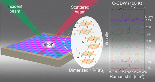
abstract = {The layered transition-metal dichalcogenide material 1T-TaS2 possesses successive phase transitions upon cooling, resulting in strong electron–electron correlation effects and the formation of charge density waves (CDWs). Recently, a dimerized double-layer stacking configuration was shown to form a Peierls-like instability in the electronic structure. To date, no direct evidence for this double-layer stacking configuration using optical techniques has been reported, in particular through Raman spectroscopy. Here, we employ a multiple excitation and polarized Raman spectroscopy to resolve the behavior of phonons and electron–phonon interactions in the commensurate CDW lattice phase of dimerized 1T-TaS2. We observe a distinct behavior from what is predicted for a single layer and probe a richer number of phonon modes that are compatible with the formation of double-layer units (layer dimerization). The multiple-excitation results show a selective coupling of each Raman-active phonon with specific electronic transitions hidden in the optical spectra of 1T-TaS2, suggesting that selectivity in the electron–phonon coupling must also play a role in the CDW order of 1T-TaS2.
},
keywords = {},
pubstate = {published},
tppubtype = {article}
}
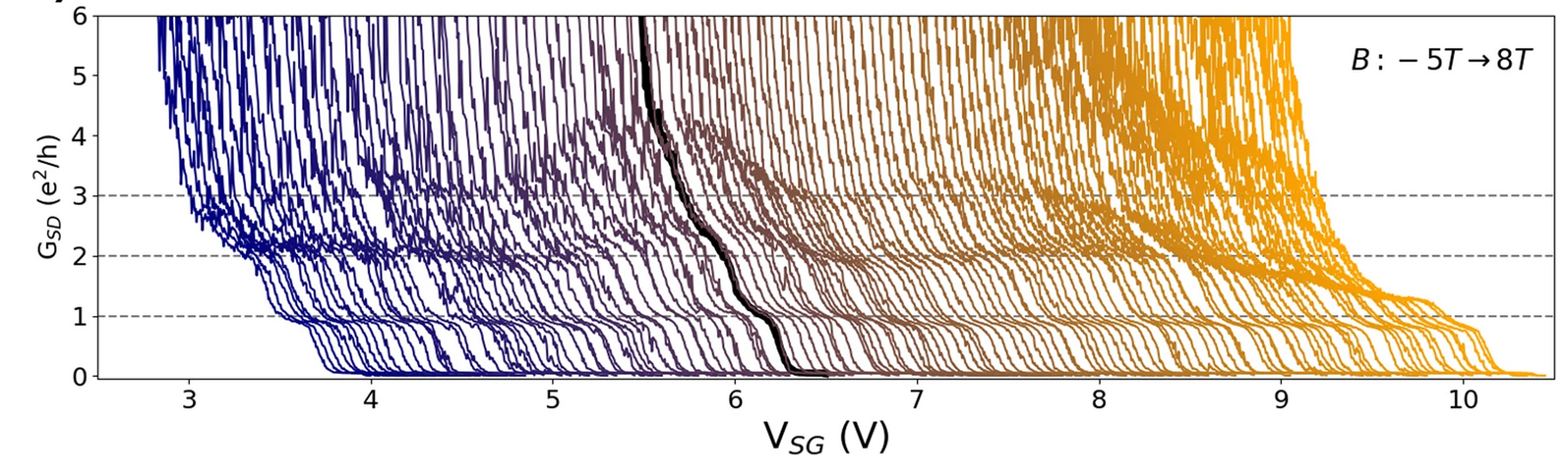
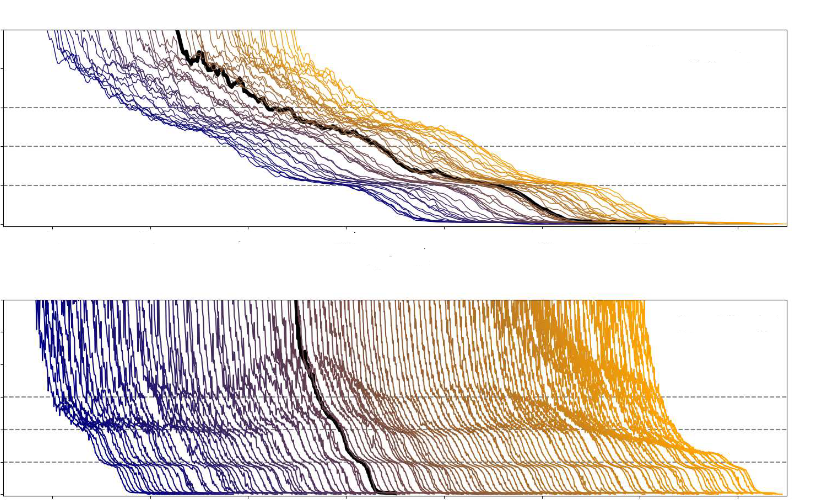
Boddison-Chouinard, Justin; Bogan, Alex; Barrios, Pedro; Lapointe, Jean; Watanabe, Kenji; Taniguchi, Takashi; Pawłowski, Jarosław; Miravet, Daniel; Bieniek, Maciej; Hawrylak, Pawel; Luican-Mayer, Adina; Gaudreau, Louis
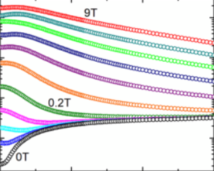
Anomalous conductance quantization of a one-dimensional channel in monolayer WSe2 Journal Article
In: npj 2D Materials and Applications, vol. 7, iss. 1, no. 50, 2023, ISBN: 2397-7132.
@article{nokey,

title = {Anomalous conductance quantization of a one-dimensional channel in monolayer WSe2},

author = {Justin Boddison-Chouinard and Alex Bogan and Pedro Barrios and Jean Lapointe and Kenji Watanabe and Takashi Taniguchi and Jarosław Pawłowski and Daniel Miravet and Maciej Bieniek and Pawel Hawrylak and Adina Luican-Mayer and Louis Gaudreau},

url = {https://doi.org/10.1038/s41699-023-00407-y},

doi = {10.1038/s41699-023-00407-y},

isbn = {2397-7132},

year  = {2023},

date = {2023-07-15},

urldate = {2023-07-15},

journal = {npj 2D Materials and Applications},

volume = {7},

number = {50},

issue = {1},

abstract = {Among quantum devices based on 2D materials, gate-defined quantum confined 1D channels are much less explored, especially in the high-mobility regime where many-body interactions play an important role. We present the results of measurements and theory of conductance quantization in a gate-defined one-dimensional channel in a single layer of transition metal dichalcogenide material WSe2. In the quasi-ballistic regime of our high-mobility sample, we report conductance quantization steps in units of e2/h for a wide range of carrier concentrations. Magnetic field measurements show that as the field is raised, higher conductance plateaus move to accurate quantized values and then shift to lower conductance values while the e2/h plateau remains locked. Based on microscopic atomistic tight-binding theory, we show that in this material, valley and spin degeneracies result in 2 e2/h conductance steps for noninteracting holes, suggesting that symmetry-breaking mechanisms such as valley polarization dominate the transport properties of such quantum structures.},

keywords = {},

pubstate = {published},

tppubtype = {article}

}
Molino, Laurent; Aggarwal, Leena; Enaldiev, Vladimir; Plumadore, Ryan; Falko, Vladimir I.; Luican-Mayer, Adina
Ferroelectric Switching at Symmetry-Broken Interfaces by Local Control of Dislocations Networks Journal Article
In: Advanced Materials, 2023, ISBN: 0935-9648.
@article{nokey,

title = {Ferroelectric Switching at Symmetry-Broken Interfaces by Local Control of Dislocations Networks},

author = {Laurent Molino and Leena Aggarwal and Vladimir Enaldiev and Ryan Plumadore and Vladimir I. Falko and Adina Luican-Mayer},

url = {https://onlinelibrary.wiley.com/doi/full/10.1002/adma.202207816

https://doi.org/10.1002/adma.202207816},

doi = {10.1002/adma.202207816},

isbn = {0935-9648},

year  = {2023},

date = {2023-06-28},

urldate = {2023-06-28},

journal = {Advanced Materials},

abstract = {Semiconducting ferroelectric materials with low energy polarization switching offer a platform for next-generation electronics such as ferroelectric

field-effect transistors. Recently discovered interfacial ferroelectricity in bilayers of transition metal dichalcogenide films provides an opportunity to

combine the potential of semiconducting ferroelectrics with the design flexibility of 2D material devices. Here, local control of ferroelectric domains in

a marginally twisted WS2 bilayer is demonstrated with a scanning tunneling microscope at room temperature, and their observed reversible evolution is

understood using a string-like model of the domain wall network (DWN). Two characteristic regimes of DWN evolution are identified: (i) elastic bending of

partial screw dislocations separating smaller domains with twin stackings due to mutual sliding of monolayers at domain boundaries and (ii) merging of

primary domain walls into perfect screw dislocations, which become the seeds for the recovery of the initial domain structure upon reversing electric

field. These results open the possibility to achieve full control over atomically thin semiconducting ferroelectric domains using local electric fields, which is

a critical step towards their technological use. },

keywords = {},

pubstate = {published},

tppubtype = {article}

}
field-effect transistors. Recently discovered interfacial ferroelectricity in bilayers of transition metal dichalcogenide films provides an opportunity to
combine the potential of semiconducting ferroelectrics with the design flexibility of 2D material devices. Here, local control of ferroelectric domains in
a marginally twisted WS2 bilayer is demonstrated with a scanning tunneling microscope at room temperature, and their observed reversible evolution is
understood using a string-like model of the domain wall network (DWN). Two characteristic regimes of DWN evolution are identified: (i) elastic bending of
partial screw dislocations separating smaller domains with twin stackings due to mutual sliding of monolayers at domain boundaries and (ii) merging of
primary domain walls into perfect screw dislocations, which become the seeds for the recovery of the initial domain structure upon reversing electric
field. These results open the possibility to achieve full control over atomically thin semiconducting ferroelectric domains using local electric fields, which is
a critical step towards their technological use.
Jimenez-Galan, Alvaro; Bossaer, Chandler; Ernotte, Guilmot; Parks, Andrew; da Silva, Rui Emanuel Ferreira; Villeneuve, David; Staudte, André; Brabec, Thomas; Luican-Mayer, Adina; Vampa, Giulio
Orbital perspective on high-harmonic generation from solids Journal Article
In: preprint, 2023.
@article{nokey,

title = {Orbital perspective on high-harmonic generation from solids},

author = {Alvaro Jimenez-Galan and Chandler Bossaer and Guilmot Ernotte and Andrew Parks and Rui Emanuel Ferreira da Silva and David Villeneuve and André Staudte and Thomas Brabec and Adina Luican-Mayer and Giulio Vampa},

url = {https://www.researchsquare.com/article/rs-2639925/v1},

doi = {https://dx.doi.org/10.21203/rs.3.rs-2639925/v1},

year  = {2023},

date = {2023-04-04},

urldate = {2023-04-04},

journal = {preprint},

abstract = {High-harmonic generation in solids allows probing and controlling electron dynamics in crystals on few femtosecond timescales, paving the way to lightwave electronics. In the spatial domain, recent advances in the real-space interpretation of high-harmonic emission in solids allows imaging the field-free, static, potential of the valence electrons with picometer resolution. The combination of such extreme spatial and temporal resolutions to measure and control strong-field dynamics in solids at the atomic scale is poised to unlock a new frontier of lightwave electronics. Here, we report a strong intensity-dependent anisotropy in the high-harmonic generation from ReS2 that we attribute to angle-dependent interference of currents from the different atoms in the unit cell. Furthermore, we demonstrate how the laser parameters control the relative contribution of these atoms to the high-harmonic emission. Our findings provide an unprecedented atomic perspective on strong-field dynamics in crystals and suggest that crystals with a large number of atoms in the unit cell are not necessarily more efficient harmonic emitters than those with fewer atoms.},

keywords = {},

pubstate = {published},

tppubtype = {article}

}
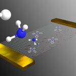
Alzate-Carvajal, Natalia; Park, Jaewoo; Bargaoui, Ilhem; Rautela, Ranjana; Comeau, Zachary J.; Scarfe, Lukas; Ménard, Jean-Michel; Darling, Seth B.; Lessard, Benoît H.; Luican-Mayer, Adina
Arrays of Functionalized Graphene Chemiresistors for Selective Sensing of Volatile Organic Compounds Journal Article
In: ACS Applied Electronic Materials, vol. 5, iss. 3, pp. 1514-1520, 2023.
@article{nokey,

title = {Arrays of Functionalized Graphene Chemiresistors for Selective Sensing of Volatile Organic Compounds},

author = {Natalia Alzate-Carvajal and Jaewoo Park and Ilhem Bargaoui and Ranjana Rautela and Zachary J. Comeau and Lukas Scarfe and Jean-Michel Ménard and Seth B. Darling and Benoît H. Lessard and Adina Luican-Mayer},

url = {https://pubs.acs.org/doi/full/10.1021/acsaelm.2c01544},

doi = {10.1021/acsaelm.2c01544     },

year  = {2023},

date = {2023-02-15},

urldate = {2023-02-15},

journal = {ACS Applied Electronic Materials},

volume = {5},

issue = {3},

pages = {1514-1520},

abstract = {Real-time detection of volatile organic compounds (VOCs) is being spotlighted for its importance in environmental monitoring and disease detection from the breath. However, the selective detection of VOCs in a small form factor gas sensor remains a challenge. Here, we present the VOC sensing performance of phthalocyanine (Pc)-functionalized graphene chemiresistors supported by the theoretical prediction of Pc’s

VOC interactions. Pc functionalization, with and without metalation, was studied parametrically with varying deposition parameters to explore impacts on the gas sensing response toward VOCs as a function of substrate coverage. Sensing data were collected to establish fingerprint signatures for a variety of VOCs. Improvement in selectivity is shown by successfully differentiating the VOCs from each other when combined into a gas sensor array tested with acetone, ethanol, formaldehyde, and toluene.},

keywords = {},

pubstate = {published},

tppubtype = {article}

}
VOC interactions. Pc functionalization, with and without metalation, was studied parametrically with varying deposition parameters to explore impacts on the gas sensing response toward VOCs as a function of substrate coverage. Sensing data were collected to establish fingerprint signatures for a variety of VOCs. Improvement in selectivity is shown by successfully differentiating the VOCs from each other when combined into a gas sensor array tested with acetone, ethanol, formaldehyde, and toluene.
2022
Luican-Mayer, Adina; Boddison-Chouinard, Justin; Bogan, Alex; Barrios, Pedro; Lapointe, Jean; Watanabe, Kenji; Taniguchia, Takashi; Pawlowski, Jaroslaw; Miravet, Daniel; Bieniek, Maciej; Hawrylak, Pawel; Gaudreau, Louis
Anomalous conductance quantization of a one-dimensional channel in monolayer WSe2 Working paper
2022.
@workingpaper{nokey,

title = {Anomalous conductance quantization of a one-dimensional channel in monolayer WSe2},

author = {Adina Luican-Mayer and Justin Boddison-Chouinard and Alex Bogan and Pedro Barrios and Jean Lapointe and Kenji Watanabe and Takashi Taniguchia and Jaroslaw Pawlowski and Daniel Miravet and Maciej Bieniek and Pawel Hawrylak and Louis Gaudreau},

url = {https://assets.researchsquare.com/files/rs-2133454/v1_covered.pdf?c=1666725261},

doi = {https://doi.org/10.21203/rs.3.rs-2133454/v1},

year  = {2022},

date = {2022-10-25},

urldate = {2022-10-25},

abstract = {Among quantum devices based on 2D materials, gate-defined quantum confined 1D channels are much less explored, especially in the high mobility regime where many body interactions play an important role. We present results of measurements and theory of conductance quantization in a gate-defined one dimensional channel in a single layer of transition metal dichalcogenide material WSe2. In the quasi-ballistic regime of our high mobility sample, we report conductance quantization steps in units of e2/h for a wide range of carrier concentrations. Magnetic field measurements show that as the field is raised higher conductance plateaus move to accurate quantized values and then

shift to lower conductance values while the e2/h plateau remains locked. Based on microscopic atomistic tight-binding theory, we show that in this material, valley and spin degeneracies result in 2 e2/h conductance steps for non-interacting holes, suggesting that symmetry breaking mechanisms such as valley polarization dominate the transport properties of such quantum structures.},

keywords = {},

pubstate = {published},

tppubtype = {workingpaper}

}
shift to lower conductance values while the e2/h plateau remains locked. Based on microscopic atomistic tight-binding theory, we show that in this material, valley and spin degeneracies result in 2 e2/h conductance steps for non-interacting holes, suggesting that symmetry breaking mechanisms such as valley polarization dominate the transport properties of such quantum structures.
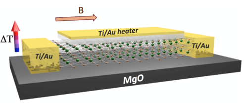
Thoutam, Laxman R.; Pate, Samuel E.; Wang, Tingting; Wang, Yong-Lei; Divan, Ralu; Martin, Ivar; Luican-Mayer, Adina; Welp, Ulrich; Kwok, Wai-Kwong; Xiao, Zhi-Li
Temperature-driven changes in the Fermi surface of graphite Journal Article
In: Phys. Rev. B, vol. 106, iss. 15, pp. 155117, 2022.
@article{PhysRevB.106.155117,

title = {Temperature-driven changes in the Fermi surface of graphite},

author = {Laxman R. Thoutam and Samuel E. Pate and Tingting Wang and Yong-Lei Wang and Ralu Divan and Ivar Martin and Adina Luican-Mayer and Ulrich Welp and Wai-Kwong Kwok and Zhi-Li Xiao},

url = {https://link.aps.org/doi/10.1103/PhysRevB.106.155117},

doi = {10.1103/PhysRevB.106.155117},

year  = {2022},

date = {2022-10-01},

urldate = {2022-10-01},

journal = {Phys. Rev. B},

volume = {106},

issue = {15},

pages = {155117},

publisher = {American Physical Society},

abstract = {We report on temperature-dependent size and anisotropy of the Fermi pockets in graphite revealed by magnetotransport measurements. The magnetoresistances (MRs) obtained in fields along the c axis obey an extended Kohler's rule, with the carrier density following the prediction of a temperature-dependent Fermi energy, indicating a change in the Fermi pocket size with temperature. The angle-dependent magnetoresistivities at a given temperature exhibit a scaling behavior. The scaling factor that reflects the anisotropy of the Fermi surface is also found to vary with temperature. Our results demonstrate that temperature-driven changes in Fermi surface can be ubiquitous and need to be considered in understanding the temperature-dependent carrier density and MR anisotropy in semimetals},

keywords = {},

pubstate = {published},

tppubtype = {article}

}
Boddison-Chouinard, Justin; Bogan, Alex; Fong, Norman; Barrios, Pedro; Lapointe, Jean; Watanabe, Kenji; Taniguchi, Takashi; Luican-Mayer, Adina; Gaudreau, Louis
Charge detection using a WSe2 van der Waals heterostructure Journal Article
In: Physical Review Applied, vol. 18, iss. 5, pp. 054017, 2022.
@article{boddison2022charge,

title = {Charge detection using a WSe2 van der Waals heterostructure},

author = {Justin Boddison-Chouinard and Alex Bogan and Norman Fong and Pedro Barrios and Jean Lapointe and Kenji Watanabe and Takashi Taniguchi and Adina Luican-Mayer and Louis Gaudreau},

url = {https://journals.aps.org/prapplied/abstract/10.1103/PhysRevApplied.18.054017

https://doi.org/10.1103/PhysRevApplied.18.054017},

doi = {18.054017},

year  = {2022},

date = {2022-03-22},

urldate = {2022-03-22},

journal = {Physical Review Applied},

volume = {18},

issue = {5},

pages = {054017},

abstract = {Charge detection is a crucial component used in semiconductor quantum circuits. It allows the noninvasive readout of charge and spin qubits in quantum information protocols and can also be leveraged for quantum sensing applications. In this work, we demonstrate that van der Waals heterostructure devices with gated nanoconstrictions in monolayer can be used as charge detectors for nearby quantum dots. This is a demonstration of charge detection using transition-metal dichalcogenides, and we find that the detection sensitivity is comparable to that of other two-dimensional (2D) material charge detectors based on graphene. These results open the possibility of implementing charge detection schemes based on 2D materials in complex quantum circuits.},

keywords = {},

pubstate = {published},

tppubtype = {article}

}

Park, Jaewoo; Jumu, Franklyn; Power, Justin; Richard, Maxime; Elsahli, Yomna; Jarkas, Mohamad Ali; Ruan, Andy; Luican-Mayer, Adina; Ménard, Jean-Michel
Drone-Mountable Gas Sensing Platform Using Graphene Chemiresistors for Remote In-Field Monitoring Journal Article
In: MDPI Sensors, vol. 22, no. 6, pp. 2383, 2022.
@article{park2022drone,

title = {Drone-Mountable Gas Sensing Platform Using Graphene Chemiresistors for Remote In-Field Monitoring},

author = {Jaewoo Park and Franklyn Jumu and Justin Power and Maxime Richard and Yomna Elsahli and Mohamad Ali Jarkas and Andy Ruan and Adina Luican-Mayer and Jean-Michel Ménard},

editor = {Olga Korostynska and Alex Mason},

doi = {https://doi.org/10.3390/s22062383},

year  = {2022},

date = {2022-03-19},

urldate = {2022-03-19},

journal = {MDPI Sensors},

volume = {22},

number = {6},

pages = {2383},

abstract = {We present the design, fabrication, and testing of a drone-mountable gas sensing platform for environmental monitoring applications. An array of graphene-based field-effect transistors in combination with commercial humidity and temperature sensors are used to relay information by wireless communication about the presence of airborne chemicals. We show that the design, based on an ESP32 microcontroller combined with a 32-bit analog-to-digital converter, can be used to achieve an electronic response similar, within a factor of two, to state-of-the-art laboratory monitoring equipment. The sensing platform is then mounted on a drone to conduct field tests, on the ground and in flight. During these tests, we demonstrate a one order of magnitude reduction in environmental noise by reducing contributions from humidity and temperature fluctuations, which are monitored in real-time with a commercial sensor integrated to the sensing platform. The sensing device is controlled by a mobile application and uses LoRaWAN, a low-power, wide-area networking protocol, for real-time data transmission to the cloud, compatible with Internet of Things (IoT) applications.},

keywords = {},

pubstate = {published},

tppubtype = {article}

}
2021
Alzate-Carvajal, Natalia; Park, Jaewoo; Pykal, Martin; Lazar, Petr; Rautela, Ranjana; Scarfe, Samantha; Scarfe, Lukas; Ménard, Jean-Michel; Otyepka, Michal; and Adina Luican-Mayer,
Graphene Field Effect Transistors: A Sensitive Platform for Detecting Sarin Journal Article
In: ACS Applied Materials & Interfaces, vol. 13, no. 51, pp. 61751-61757, 2021.
@article{Alzate-Carvajal2021,

title = {Graphene Field Effect Transistors: A Sensitive Platform for Detecting Sarin},

author = {Natalia Alzate-Carvajal and Jaewoo Park and Martin Pykal and Petr Lazar and Ranjana Rautela and Samantha Scarfe and Lukas Scarfe and Jean-Michel Ménard and Michal Otyepka and and Adina Luican-Mayer},

doi = {https://doi.org/10.1021/acsami.1c17770},

year  = {2021},

date = {2021-12-15},

urldate = {2021-12-15},

journal = {ACS Applied Materials & Interfaces},

volume = {13},

number = {51},

pages = {61751-61757},

abstract = {Real time, rapid, and accurate detection of chemical warfare agents (CWA) is an ongoing security challenge. Typical detection methods for CWA are adapted from traditional chemistry techniques such as chromatography and mass spectrometry, which lack portability. Here, we address this challenge by evaluating graphene field effect transistors (GFETs) as a sensing platform for sarin gas using both experiment and theory. Experimentally, we measure the sensing response of GFETs when exposed to dimethyl methylphosphonate (DMMP), a less toxic compound used as simulant due to its chemical similarities to sarin. We find low detection limits of 800 ppb, the highest sensitivity reported up to date for this type of sensing platform. In addition to changes in resistance, we implement an in-operando monitor of the GFETs characteristics during and after exposure to the analyte, which gives insights into the graphene–DMMP interactions. Moreover, using theoretical calculations, we show that DMMP and sarin interact similarly with graphene, implying that GFETs should be highly sensitive to detecting sarin. GFETs offer a versatile platform for the development of compact and miniaturized devices that can provide real-time detection of dangerous chemicals in the local environment.},

keywords = {},

pubstate = {published},

tppubtype = {article}

}
Park, Jaewoo; Rautela, Ranjana; Alzate-Carvajal, Natalia; Scarfe, Samantha; Scarfe, Lukas; Alarie, Luc; Luican-Mayer, Adina; and Jean-Michel Ménard,
UV Illumination as a Method to Improve the Performance of Gas Sensors Based on Graphene Field-Effect Transistors Journal Article
In: ACS Sensors, vol. 6, no. 12, pp. 4417-4424, 2021.
@article{Park2021,

title = {UV Illumination as a Method to Improve the Performance of Gas Sensors Based on Graphene Field-Effect Transistors},

author = {Jaewoo Park and Ranjana Rautela and Natalia Alzate-Carvajal and Samantha Scarfe and Lukas Scarfe and Luc Alarie and Adina Luican-Mayer and and Jean-Michel Ménard},

doi = {https://doi.org/10.1021/acssensors.1c01783},

year  = {2021},

date = {2021-11-18},

urldate = {2021-11-18},

journal = {ACS Sensors},

volume = {6},

number = {12},

pages = {4417-4424},

abstract = {The ability to detect and recognize airborne chemical species is essential to enable applications in security, health, and environmental monitoring. Here, we report a sensing platform based on graphene field-effect transistor (GFET) devices combined with optical illumination for the detection of volatile compounds. We compare the change in resistance of GFET sensors upon exposure to analytes such as ethanol, dimethyl methylphosphonate (DMMP), and water vapors with and without the presence of a local illuminating ultraviolet (UV) light-emitting diode (LED). Our results show that UV illumination acts as a control knob for the electronic transport properties of graphene, increasing the device’s response to ethanol, water, and DMMP, up to a factor of 54, and enabling ppb-level detection of DMMP at 800 ppb without chemical functionalization of the graphene layer. The sensing response can be optimized to reveal an analyte-specific interplay between the induced changes in carrier concentration and mobility of the GFET. These findings provide a pathway to enhancing the sensitivity of GFET sensors and a differentiation channel to improve their selectivity.},

keywords = {},

pubstate = {published},

tppubtype = {article}

}
Boddison-Chouinard, Justin; Bogan, Alex; Fong, Norman; Watanabe, Kenji; Taniguchi, Takashi; Studenikin, Sergei; Sachrajda, Andrew; Korkusinski, Marek; Altintas, Abdulmenaf; Bieniek, Maciej; Hawrylak, Pawel; Luican-Mayer, Adina; Gaudreau, Louis
Gate controlled quantum dots in monolayer WSe2 Journal Article
In: Applied Physics Letters, vol. 119, pp. 133104, 2021.
@article{Chouinard2021,

title = {Gate controlled quantum dots in monolayer WSe2},

author = {Justin Boddison-Chouinard and Alex Bogan and Norman Fong and Kenji Watanabe and Takashi Taniguchi and Sergei Studenikin and Andrew Sachrajda and Marek Korkusinski and Abdulmenaf Altintas and Maciej Bieniek and Pawel Hawrylak and Adina Luican-Mayer and Louis Gaudreau},

doi = {https://doi.org/10.1063/5.0062838},

year  = {2021},

date = {2021-09-28},

urldate = {2021-09-28},

journal = {Applied Physics Letters},

volume = {119},

pages = {133104},

abstract = {Quantum confinement and manipulation of charge carriers are critical for achieving devices practical for quantum technologies. The interplay between electron spin and valley, as well as the possibility to address their quantum states electrically and optically, makes two-dimensional (2D) transition metal dichalcogenides an emerging platform for the development of quantum devices. In this work, we fabricate devices based on heterostructures of layered 2D materials, in which we realize gate-controlled tungsten diselenide (WSe2) hole quantum dots. We discuss the observed mesoscopic transport features related to the emergence of quantum dots in the WSe2 device channel, and we compare them to a theoretical model.},

keywords = {},

pubstate = {published},

tppubtype = {article}

}
Scarfe, Samantha; Cui, Wei; Luican-Mayer, Adina; Ménard, Jean-Michel
Systematic THz study of the substrate effect in limiting the mobility of graphene Journal Article
In: Nature Scientific Reports, vol. 11, pp. 8729, 2021.
@article{Scarfe2021,

title = {Systematic THz study of the substrate effect in limiting the mobility of graphene},

author = {Samantha Scarfe and Wei Cui and Adina Luican-Mayer and Jean-Michel Ménard},

url = {https://www.nature.com/articles/s41598-021-87894-5},

doi = {https://doi.org/10.1038/s41598-021-87894-5},

year  = {2021},

date = {2021-04-22},

urldate = {2021-04-22},

journal = {Nature Scientific Reports},

volume = {11},

pages = {8729},

abstract = {We explore the substrate-dependent charge carrier dynamics of large area graphene films using contact-free non-invasive terahertz spectroscopy. The graphene samples are deposited on seven distinct substrates relevant to semiconductor technologies and flexible/photodetection devices. Using a Drude model for Dirac fermions in graphene and a fitting method based on statistical signal analysis, we extract transport properties such as the charge carrier density and carrier mobility. We find that graphene films supported by substrates with minimal charged impurities exhibit an enhanced carrier mobility, while substrates with a high surface roughness generally lead to a lower transport performance. The smallest amount of doping is observed for graphene placed on the polymer Zeonor, which also has the highest carrier mobility. This work provides valuable guidance in choosing an optimal substrate for graphene to enable applications where high mobility is required.},

keywords = {},

pubstate = {published},

tppubtype = {article}

}
Ménard, Jean-Michel; Luican-Mayer, Adina; Rautela, Ranjana
Illuminated ultra-thin chemical sensors, and systems and methods comprising same Patent
2021.
@patent{US16949135,

title = {Illuminated ultra-thin chemical sensors, and systems and methods comprising same},

author = {Jean-Michel Ménard and Adina Luican-Mayer and Ranjana Rautela},

url = {https://patentimages.storage.googleapis.com/fd/35/9c/e33edb599f3f5e/US20210109054A1.pdf},

year  = {2021},

date = {2021-04-15},

abstract = {Described are various embodiments of a system and method for selectively identifying the presence of a designated chemical species within a chemical sample using a two-dimensional sensor, which, when exposed to illumination, provides a differentiable adsorption sensor response signal for chemical identification.},

howpublished = {US16949135},

keywords = {},

pubstate = {published},

tppubtype = {patent}

}
2020

Plumadore, Ryan; Baskurt, Mehmet; Boddison-Chouinard, Justin; Lopinski, Gregory; Modarresi, Mohsen; Potasz, Pawel; Hawrylak, Pawel; Sahin, Hasan; Peeters, Francois M.; Luican-Mayer, Adina
Prevalence of oxygen defects in an in-plane anisotropic transition metal dichalcogenide Journal Article
In: Phys. Rev. B, vol. 102, no. 20, pp. 205408, 2020.
@article{Plumadore2020,

title = {Prevalence of oxygen defects in an in-plane anisotropic transition metal dichalcogenide},

author = {Ryan Plumadore and Mehmet Baskurt and Justin Boddison-Chouinard and Gregory Lopinski and Mohsen Modarresi and Pawel Potasz and Pawel Hawrylak and Hasan Sahin and Francois M. Peeters and Adina Luican-Mayer},

doi = {doi.org/10.1103/PhysRevB.102.205408},

year  = {2020},

date = {2020-11-09},

urldate = {2020-11-09},

journal = {Phys. Rev. B},

volume = {102},

number = {20},

pages = {205408},

abstract = {Atomic scale defects in semiconductors enable their technological applications and realization of different quantum states. Using scanning tunneling microscopy and spectroscopy complemented by ab initio calculations we determine the nature of defects in the anisotropic van der Waals layered semiconductor ReS2. We demonstrate the in-plane anisotropy of the lattice by directly visualizing chains of rhenium atoms forming diamond-shaped clusters. Using scanning tunneling spectroscopy we measure the semiconducting gap in the density of states. We reveal the presence of lattice defects and by comparison of their topographic and spectroscopic signatures with ab initio calculations we determine their origin as oxygen atoms absorbed at lattice point defect sites. These results provide an atomic-scale view into the semiconducting transition metal dichalcogenides, paving the way toward understanding and engineering their properties.},

keywords = {},

pubstate = {published},

tppubtype = {article}

}
Alzate-Carvajal, Natalia; Luican-Mayer, Adina
Functionalized Graphene Surfaces for Selective Gas Sensing Journal Article
In: ACS Omega, vol. 5, iss. 34, pp. 21320 - 21329, 2020, ISBN: 2470-1343.
@article{Alzate-Carvajal2020,

title = {Functionalized Graphene Surfaces for Selective Gas Sensing},

author = { Natalia Alzate-Carvajal and Adina Luican-Mayer },

url = {https://pubs.acs.org/doi/10.1021/acsomega.0c02861},

doi = {10.1021/acsomega.0c02861},

isbn = {2470-1343},

year  = {2020},

date = {2020-09-01},

urldate = {2020-08-21},

journal = {ACS Omega},

volume = {5},

issue = {34},

pages = {21320 - 21329},

publisher = {American Chemical Society},

abstract = {Environmental monitoring through gas sensors is paramount for the safety and security of industrial workers and for ecological protection. Graphene is among the most promising materials considered for next-generation gas sensing due to its properties such as mechanical strength and flexibility, high surface-to-volume ratio, large conductivity, and low electrical noise. While gas sensors based on graphene devices have already demonstrated high sensitivity, one of the most important figures of merit, selectivity, remains a challenge. In the past few years, however, surface functionalization emerged as a potential route to achieve selectivity. This review surveys the recent advances in the fabrication and characterization of graphene and reduced graphene oxide gas sensors chemically functionalized with aromatic molecules and polymers with the goal of improving selectivity toward specific gases as well as overall sensor performance.},

keywords = {},

pubstate = {published},

tppubtype = {article}

}
Rautela, Ranjana; Scarfe, Samantha; Guay, Jean-Michel; Lazar, Petr; Pykal, Martin; Azimi, Saied; Grenapin, Cedric; Boddison-Chouinard, Justin; Halpin, Alexei; Wang, Weixiang; Andrzejewski, Lukasz; Plumadore, Ryan; Park, Jeongwon; Menard, Jean-Michel; Otyepka, Michal; Luican-Mayer, Adina
Mechanistic insight into the limiting factors of graphene-based environmental sensors Journal Article
In: ACS Applied Materials & Interfaces, 2020, ISSN: 1944-8244.
@article{Rautela2020,

title = {Mechanistic insight into the limiting factors of graphene-based environmental sensors},

author = {Ranjana Rautela and Samantha Scarfe and Jean-Michel Guay and Petr Lazar and Martin Pykal and Saied Azimi and Cedric Grenapin and Justin Boddison-Chouinard and Alexei Halpin and Weixiang Wang and Lukasz Andrzejewski and Ryan Plumadore and Jeongwon Park and Jean-Michel Menard and Michal Otyepka and Adina Luican-Mayer},

url = {https://doi.org/10.1021/acsami.0c09051},

doi = {10.1021/acsami.0c09051},

issn = {1944-8244},

year  = {2020},

date = {2020-07-13},

journal = {ACS Applied Materials & Interfaces},

publisher = {American Chemical Society},

abstract = {Graphene has demonstrated great promise for technological use, yet control over material growth and understanding of how material imperfections affect the performance of devices are challenges that hamper the development of applications. In this work we reveal new insight into the connections between the performance of the graphene devices as environmental sensors and the microscopic details of the interactions at the sensing surface. We monitor changes in the resistance of the chemical-vapour deposition grown graphene devices as exposed to different concentrations of ethanol. We perform thermal surface treatments after the devices are fabricated, use scanning probe microscopy to visualize their effects down to nanometer scale and correlate them with the measured performance of the device as an ethanol sensor. Our observations are compared to theoretical calculations of charge transfers between molecules and the graphene surface. We find that, although often overlooked, the surface cleanliness after device fabrication is responsible for the device performance and reliability. These results further our understanding of the mechanisms of sensing in graphene-based environmental sensors and pave the way to optimizing such devices, especially for their miniaturization, as with decrising size of the active zone the potential role of contaminants will rise.},

keywords = {},

pubstate = {published},

tppubtype = {article}

}
Plumadore, Ryan; Ezzi, Mohammed M Al; Adam, Shaffique; Luican-Mayer, Adina
Moiré patterns in graphene–rhenium disulfide vertical heterostructures Journal Article
In: Journal of Applied Physics, vol. 128, no. 4, pp. 044303, 2020.
@article{doi:10.1063/5.0015643,

title = {Moiré patterns in graphene–rhenium disulfide vertical heterostructures},

author = {Ryan Plumadore and Mohammed M Al Ezzi and Shaffique Adam and Adina Luican-Mayer},

url = {https://doi.org/10.1063/5.0015643},

doi = {10.1063/5.0015643},

year  = {2020},

date = {2020-01-01},

journal = {Journal of Applied Physics},

volume = {128},

number = {4},

pages = {044303},

abstract = {Vertical stacking of atomically thin materials offers a large platform for realizing novel properties enabled by proximity effects and moiré patterns. Here, we focus on mechanically assembled heterostructures of graphene and ReS2, a van der Waals layered semiconductor. Using scanning tunneling microscopy and spectroscopy, we image the sharp edge between the two materials as well as areas of overlap. Locally resolved topographic images revealed the presence of a striped superpattern originating in the interlayer interactions between graphene's hexagonal structure and the triclinic, low in-plane symmetry of ReS2. We compare the results with a theoretical model that estimates the shape and angle dependence of the moiré pattern between graphene and ReS2. These results shed light on the complex interface phenomena between van der Waals materials with different lattice symmetries.},

keywords = {},

pubstate = {published},

tppubtype = {article}

}
2019
Ramos, Sergio L. L. M.; Plumadore, Ryan; Boddison-Chouinard, Justin; Hla, Saw Wai; Guest, Jeffrey R.; Gosztola, David J.; Pimenta, Marcos A.; Luican-Mayer, Adina
Suppression of the commensurate charge density wave phase in ultrathin 1T- TaS2 evidenced by Raman hyperspectral analysis Journal Article
In: Physical Review B, vol. 100, no. 16, pp. 165414, 2019.
@article{ramos2019suppression,

title = {Suppression of the commensurate charge density wave phase in ultrathin 1T- TaS2 evidenced by Raman hyperspectral analysis},

author = {Sergio L. L. M. Ramos and Ryan Plumadore and Justin Boddison-Chouinard and Saw Wai Hla and Jeffrey R. Guest and David J. Gosztola and Marcos A. Pimenta and Adina Luican-Mayer},

url = {https://link.aps.org/doi/10.1103/PhysRevB.100.165414},

doi = {10.1103/PhysRevB.100.165414},

year  = {2019},

date = {2019-10-21},

urldate = {2019-10-21},

journal = {Physical Review B},

volume = {100},

number = {16},

pages = {165414},

publisher = {APS},

abstract = {Using temperature-dependent and low-frequency Raman spectroscopy, we address the question of how the transition from bulk to a few atomic layers affects the charge density wave (CDW) phases in 1T−TaS2. We find that for crystals with thickness larger than ≈10 nm the transition temperatures between the different phases as well as the hysteresis that occurs in the thermal cycle correspond to the ones expected for a bulk sample. However, when the crystals become thinner than ≈10 nm, the low-temperature commensurate CDW phases can be suppressed down to the experimentally accessible temperatures (∼80 K) upon cooling at moderate rates (∼5Kmin−1). In addition, even the near commensurate CDW phase is not accessible in few-layer flakes below ≈4 nm for even slower cooling rates (∼1Kmin−1). We employ Raman hyperspectral imaging to statistically confirm these findings and consider the interlayer coupling and its dynamics to play significant roles in determining the properties of CDW systems consisting of a few unit cells in the vertical direction.},

keywords = {},

pubstate = {published},

tppubtype = {article}

}
Boddison-Chouinard, Justin; Scarfe, Samantha; Watanabe, K; Taniguchi, T; Luican-Mayer, Adina
Flattening van der Waals heterostructure interfaces by local thermal treatment Journal Article
In: Applied Physics Letters, vol. 115, no. 23, pp. 231603, 2019.
@article{boddison2019flattening,

title = {Flattening van der Waals heterostructure interfaces by local thermal treatment},

author = {Justin Boddison-Chouinard and Samantha Scarfe and K Watanabe and T Taniguchi and Adina Luican-Mayer},

url = {https://doi.org/10.1063/1.5131022},

doi = {10.1063/1.5131022},

year  = {2019},

date = {2019-01-01},

journal = {Applied Physics Letters},

volume = {115},

number = {23},

pages = {231603},

publisher = {AIP Publishing LLC},

abstract = {Fabrication of custom-built heterostructures based on stacked 2D materials provides an effective method to controllably tune electronic and optical properties. To that end, optimizing fabrication techniques for building these heterostructures is imperative. A common challenge in layer-by-layer assembly of 2D materials is the formation of bubbles at atomically thin interfaces. We propose a technique for addressing this issue by removing the bubbles formed at the heterostructure interface in a custom-defined area using the heat generated by a laser equipped with raster scanning capabilities. We demonstrate that the density of bubbles formed at graphene-ReS2 interfaces can be controllably reduced using this method. We discuss an understanding of the flattening mechanism by considering the interplay of interface thermal conductivities and adhesion energies between two atomically thin 2D materials.

The authors acknowledge funding from the National Sciences and Engineering Research Council (NSERC) Discovery Grant No. RGPIN-2016-06717. We also acknowledge the support of the Natural Sciences and Engineering Research Council of Canada (NSERC) through Strategic Project No. STPGP 521420 (Quantum Circuits in 2D materials). Growth of hexagonal boron nitride crystals (K.W. and T.T.) was supported by the Elemental Strategy Initiative conducted by the MEXT, Japan, and the CREST (No. JPMJCR15F3), J.S.T. We thank Professor Jean-Michel Menard and Professor Rui Huang for useful discussions and Emmanuelle Launay for technical support.},

keywords = {},

pubstate = {published},

tppubtype = {article}

}
The authors acknowledge funding from the National Sciences and Engineering Research Council (NSERC) Discovery Grant No. RGPIN-2016-06717. We also acknowledge the support of the Natural Sciences and Engineering Research Council of Canada (NSERC) through Strategic Project No. STPGP 521420 (Quantum Circuits in 2D materials). Growth of hexagonal boron nitride crystals (K.W. and T.T.) was supported by the Elemental Strategy Initiative conducted by the MEXT, Japan, and the CREST (No. JPMJCR15F3), J.S.T. We thank Professor Jean-Michel Menard and Professor Rui Huang for useful discussions and Emmanuelle Launay for technical support.
Luican-Mayer, Adina; Zhang, Yuan; DiLullo, Andrew; Li, Yang; Fisher, Brandon; Ulloa, Sergio E; Hla, Saw-Wai
Negative differential resistance observed on the charge density wave of a transition metal dichalcogenide Journal Article
In: Nanoscale, vol. 11, no. 46, pp. 22351–22358, 2019.
@article{luican2019negative,

title = {Negative differential resistance observed on the charge density wave of a transition metal dichalcogenide},

author = {Adina Luican-Mayer and Yuan Zhang and Andrew DiLullo and Yang Li and Brandon Fisher and Sergio E Ulloa and Saw-Wai Hla},

url = {http://dx.doi.org/10.1039/C9NR07857F},

doi = {10.1039/C9NR07857F},

year  = {2019},

date = {2019-01-01},

journal = {Nanoscale},

volume = {11},

number = {46},

pages = {22351--22358},

publisher = {Royal Society of Chemistry},

abstract = {Charge density waves and negative differential resistance are seemingly unconnected physical phenomena. The former is an ordered quantum fluid of electrons{,} intensely investigated for its relation with superconductivity{,} while the latter receives much attention for its potential applications in electronics. Here we show that these two phenomena can not only coexist but also that the localized electronic states of the charge density wave are essential to induce negative differential resistance in a transition metal dichalcogenide{,} 1T-TaS2. Using scanning tunneling microscopy and spectroscopy{,} we report the observation of negative differential resistance in the commensurate charge density wave state of 1T-TaS2. The observed phenomenon is explained by the interplay of interlayer and intra-layer tunneling with the participation of the atomically localized states of the charge density wave maxima and minima. We demonstrate that lattice defects can locally affect the coupling between the layers and are therefore a mechanism to realize NDR in these materials.},

keywords = {},

pubstate = {published},

tppubtype = {article}

}
Stecher, Kristen; Huang, Symphony Hsiao-Yuan; Escorcio, Rodrigo; Luican-Mayer, Adina
Demonstrating the concepts of sheet resistance, field effect, and mobility of a semiconductor using graphene field effect transistors Journal Article
In: European Journal of Physics, vol. 40, no. 6, pp. 065501, 2019.
@article{stecher2019demonstrating,

title = {Demonstrating the concepts of sheet resistance, field effect, and mobility of a semiconductor using graphene field effect transistors},

author = {Kristen Stecher and Symphony Hsiao-Yuan Huang and Rodrigo Escorcio and Adina Luican-Mayer},

url = {https://doi.org/10.1088%2F1361-6404%2Fab4444},

doi = {10.1088/1361-6404/ab4444},

year  = {2019},

date = {2019-01-01},

journal = {European Journal of Physics},

volume = {40},

number = {6},

pages = {065501},

publisher = {IOP Publishing},

abstract = {With rapid advancement in the discovery of innovative materials, there is great opportunity for enhancing undergraduate laboratories teaching basic physics. Here, we exemplify a laboratory focused on basic concepts of semiconductors (sheet resistance, field effect, mobility) taking advantage of commercially available graphene devices, a cutting-edge material system. We present an experimental set-up and protocol that can be used to implement such a laboratory lecture. We introduce the physics concepts that will be explored and we discuss the results obtained when we carried out the described laboratory experiment.},

keywords = {},

pubstate = {published},

tppubtype = {article}

}
Luican-Mayer, Adina
A needle in a moiré stack Journal Article
In: Nature Physics, vol. 15, no. 11, pp. 1107–1108, 2019.
@article{luican2019needle,

title = {A needle in a moiré stack},

author = {Adina Luican-Mayer},

url = {https://doi.org/10.1038/s41567-019-0645-y},

doi = {10.1038/s41567-019-0645-y},

year  = {2019},

date = {2019-01-01},

journal = {Nature Physics},

volume = {15},

number = {11},

pages = {1107--1108},

publisher = {Nature Publishing Group},

abstract = {Spatially resolved measurements of twisted bilayer graphene reveal more details of the strongly correlated electrons.},

keywords = {},

pubstate = {published},

tppubtype = {article}

}
Boddison-Chouinard, Justin; Plumadore, Ryan; Luican-Mayer, Adina
Fabricating van der Waals Heterostructures with Precise Rotational Alignment Journal Article
In: JoVE (Journal of Visualized Experiments), no. 149, pp. e59727, 2019.
@article{boddison2019fabricating,

title = {Fabricating van der Waals Heterostructures with Precise Rotational Alignment},

author = {Justin Boddison-Chouinard and Ryan Plumadore and Adina Luican-Mayer},

url = {https://europepmc.org/article/med/31329181},

doi = {10.3791/59727},

year  = {2019},

date = {2019-01-01},

journal = {JoVE (Journal of Visualized Experiments)},

number = {149},

pages = {e59727},

abstract = {In this work we describe a technique for creating new crystals (van der Waals heterostructures) by stacking distinct ultrathin layered 2D materials. We demonstrate not only lateral control but, importantly, also control over the angular alignment of adjacent layers. The core of the technique is represented by a home-built transfer setup which allows the user to control the position of the individual crystals involved in the transfer. This is achieved with sub-micrometer (translational) and sub-degree (angular) precision. Prior to stacking them together, the isolated crystals are individually manipulated by custom-designed moving stages that are controlled by a programmed software interface. Moreover, since the entire transfer setup is computer controlled, the user can remotely create precise heterostructures without coming into direct contact with the transfer setup, labeling this technique as "hands-free". In addition to presenting the transfer set-up, we also describe two techniques for preparing the crystals that are subsequently stacked.},

keywords = {},

pubstate = {published},

tppubtype = {article}

}
2017
Wu, Stephen M; Luican-Mayer, Adina; Bhattacharya, Anand
Nanoscale measurement of Nernst effect in two-dimensional charge density wave material 1T-TaS2 Journal Article
In: Applied Physics Letters, vol. 111, no. 22, pp. 223109, 2017.
@article{wu2017nanoscale,

title = {Nanoscale measurement of Nernst effect in two-dimensional charge density wave material 1T-TaS2},

author = {Stephen M Wu and Adina Luican-Mayer and Anand Bhattacharya},

url = {https://doi.org/10.1063/1.5004804},

year  = {2017},

date = {2017-01-01},

urldate = {2017-01-01},

journal = {Applied Physics Letters},

volume = {111},

number = {22},

pages = {223109},

publisher = {AIP Publishing LLC},

abstract = {Advances in nanoscale material characterization on two-dimensional van der Waals layered materials primarily involve their optical and electronic properties. The thermal properties of these materials are harder to access due to the difficulty of thermal measurements at the nanoscale. In this work, we create a nanoscale magnetothermal device platform to access the basic out-of-plane magnetothermal transport properties of ultrathin van der Waals materials. Specifically, the Nernst effect in the charge density wave transition metal dichalcogenide 1T-TaS2 is examined on nano-thin flakes in a patterned device structure. It is revealed that near the commensurate charge density wave (CCDW) to nearly commensurate charge density wave (NCCDW) phase transition, the polarity of the Nernst effect changes. Since the Nernst effect is especially sensitive to changes in the Fermi surface, this suggests that large changes are occurring in the out-of-plane electronic structure of 1T-TaS2, which are otherwise unresolved in just in-plane electronic transport measurements. This may signal a coherent evolution of out-of-plane stacking in the CCDW → NCCDW transition.

All authors acknowledge support of the U.S. Department of Energy (DOE), Office of Science, Basic Energy Sciences (BES), Materials Sciences and Engineering Division. The use of facilities at the Center for Nanoscale Materials was supported by the U.S. DOE, BES under Contract No. DE-AC02-06CH11357.},

keywords = {},

pubstate = {published},

tppubtype = {article}

}
All authors acknowledge support of the U.S. Department of Energy (DOE), Office of Science, Basic Energy Sciences (BES), Materials Sciences and Engineering Division. The use of facilities at the Center for Nanoscale Materials was supported by the U.S. DOE, BES under Contract No. DE-AC02-06CH11357.
Luican-Mayer, Adina; Li, Guohong; Andrei, Eva Y
Atomic scale characterization of mismatched graphene layers Journal Article
In: Journal of Electron Spectroscopy and Related Phenomena, vol. 219, pp. 92–98, 2017.
@article{luican2017atomic,

title = {Atomic scale characterization of mismatched graphene layers},

author = {Adina Luican-Mayer and Guohong Li and Eva Y Andrei},

url = {http://www.sciencedirect.com/science/article/pii/S0368204817300269},

doi = {https://doi.org/10.1016/j.elspec.2017.01.005},

year  = {2017},

date = {2017-01-01},

journal = {Journal of Electron Spectroscopy and Related Phenomena},

volume = {219},

pages = {92--98},

publisher = {Elsevier},

abstract = {In the bourgeoning field of two dimensional layered materials and their atomically thin counterparts, it has been established that the electronic coupling between the layers of the material plays a key role in determining its properties [1,2]. We are just beginning to understand how each material is unique in that respect while working our way up to building new materials with functionalities enabled by interlayer interactions. In this review, we will focus on a system that despite its apparent simplicity possesses a wealth of intriguing physics: layers of graphene with various degree of coupling. The situations discussed here are graphene layers vertically twisted with respect with each other, weakly decoupled electronically and laterally twisted forming grain boundaries. We emphasize experiments that atomically resolve the electronic properties.},

keywords = {},

pubstate = {published},

tppubtype = {article}

}
2016
Luican-Mayer, Adina; Barrios-Vargas, Jose E; Falkenberg, Jesper Toft; Autès, Gabriel; Cummings, Aron W; Soriano, David; Li, Guohong; Brandbyge, Mads; Yazyev, Oleg V; Roche, Stephan; others,
Localized electronic states at grain boundaries on the surface of graphene and graphite Journal Article
In: 2D Materials, vol. 3, no. 3, pp. 031005, 2016.
@article{luican2016localized,

title = {Localized electronic states at grain boundaries on the surface of graphene and graphite},

author = {Adina Luican-Mayer and Jose E Barrios-Vargas and Jesper Toft Falkenberg and Gabriel Autès and Aron W Cummings and David Soriano and Guohong Li and Mads Brandbyge and Oleg V Yazyev and Stephan Roche and others},

url = {https://doi.org/10.1088%2F2053-1583%2F3%2F3%2F031005},

doi = {10.1088/2053-1583/3/3/031005},

year  = {2016},

date = {2016-08-12},

urldate = {2016-01-01},

journal = {2D Materials},

volume = {3},

number = {3},

pages = {031005},

publisher = {IOP Publishing},

abstract = {Recent advances in large-scale synthesis of graphene and other 2D materials have underscored the importance of local defects such as dislocations and grain boundaries (GBs), and especially their tendency to alter the electronic properties of the material. Understanding how the polycrystalline morphology affects the electronic properties is crucial for the development of applications such as flexible electronics, energy harvesting devices or sensors. We here report on atomic scale characterization of several GBs and on the structural-dependence of the localized electronic states in their vicinity. Using low temperature scanning tunneling microscopy  and spectroscopy, together with tight binding and ab initio numerical simulations we explore GBs on the surface of graphite and elucidate the interconnection between the local density of states and their atomic structure. We show that the electronic fingerprints of these GBs consist of pronounced resonances which, depending on the relative orientation of the adjacent crystallites, appear either on the electron side of the spectrum or as an electron-hole symmetric doublet close to the charge neutrality point. These two types of spectral features will impact very differently the transport properties allowing, in the asymmetric case to introduce transport anisotropy which could be utilized to design novel growth and fabrication strategies to control device performance.},

keywords = {},

pubstate = {published},

tppubtype = {article}

}
Lu, Chih-Pin; Rodriguez-Vega, Martin; Li, Guohong; Luican-Mayer, Adina; Watanabe, Kenji; Taniguchi, Takashi; Rossi, Enrico; Andrei, Eva Y
Local, global, and nonlinear screening in twisted double-layer graphene Journal Article
In: Proceedings of the National Academy of Sciences, vol. 113, no. 24, pp. 6623–6628, 2016.
@article{lu2016local,

title = {Local, global, and nonlinear screening in twisted double-layer graphene},

author = {Chih-Pin Lu and Martin Rodriguez-Vega and Guohong Li and Adina Luican-Mayer and Kenji Watanabe and Takashi Taniguchi and Enrico Rossi and Eva Y Andrei},

url = {https://www.pnas.org/content/113/24/6623/tab-article-info},

doi = {https://doi.org/10.1073/pnas.1606278113},

year  = {2016},

date = {2016-01-01},

journal = {Proceedings of the National Academy of Sciences},

volume = {113},

number = {24},

pages = {6623--6628},

publisher = {National Acad Sciences},

abstract = {One-atom-thick crystalline layers and their vertical heterostructures carry the promise of designer electronic materials that are unattainable by standard growth techniques. To realize their potential it is necessary to isolate them from environmental disturbances, in particular those introduced by the substrate. However, finding and characterizing suitable substrates, and minimizing the random potential fluctuations they introduce, has been a persistent challenge in this emerging field. Here we show that Landau-level (LL) spectroscopy offers the unique capability to quantify both the reduction of the quasiparticles’ lifetime and the long-range inhomogeneity due to random potential fluctuations. Harnessing this technique together with direct scanning tunneling microscopy and numerical simulations we demonstrate that the insertion of a graphene buffer layer with a large twist angle is a very effective method to shield a 2D system from substrate interference that has the additional desirable property of preserving the electronic structure of the system under study. We further show that owing to its remarkable nonlinear screening capability a single graphene buffer layer provides better shielding than either increasing the distance to the substrate or doubling the carrier density and reduces the amplitude of the potential fluctuations in graphene to values even lower than the ones in AB-stacked bilayer graphene.},

keywords = {},

pubstate = {published},

tppubtype = {article}

}
2015
Thoutam, L. R.; Wang, Y. L.; Xiao, Z. L.; Das, S.; Luican-Mayer, A.; Divan, R.; Crabtree, G. W.; Kwok, W. K.
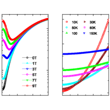
Temperature-dependent three-dimensional anisotropy of the magnetoresistance in WTe2 Journal Article
In: Physical review letters, vol. 115, no. 4, pp. 046602, 2015.
@article{thoutam2015temperature,

title = {Temperature-dependent three-dimensional anisotropy of the magnetoresistance in WTe2},

author = {L.R. Thoutam and Y.L. Wang and Z.L. Xiao and S. Das and A. Luican-Mayer and R. Divan and G.W. Crabtree and W.K. Kwok},

url = {https://link.aps.org/doi/10.1103/PhysRevLett.115.046602},

doi = {10.1103/PhysRevLett.115.046602},

year  = {2015},

date = {2015-07-22},

urldate = {2015-07-22},

journal = {Physical review letters},

volume = {115},

number = {4},

pages = {046602},

publisher = {APS},

abstract = {Extremely large magnetoresistance (XMR) was recently discovered in WTe2, triggering extensive research on this material regarding the XMR origin. Since WTe2 is a layered compound with metal layers sandwiched between adjacent insulating chalcogenide layers, this material has been considered to be electronically two-dimensional (2D). Here we report two new findings on WTe2: (1) WTe2 is electronically 3D with a mass anisotropy as low as 2, as revealed by the 3D scaling behavior of the resistance R(H,θ)=R(ϵθH) with ϵθ=(cos2θ+γ−2sin2θ)1/2, θ being the magnetic field angle with respect to the c axis of the crystal and γ  being the mass anisotropy and (2) the mass anisotropy γ varies with temperature and follows the magnetoresistance behavior of the Fermi liquid state. Our results not only provide a general scaling approach for the anisotropic magnetoresistance but also are crucial for correctly understanding the electronic properties of WTe2, including the origin of the remarkable “turn-on” behavior in the resistance versus temperature curve, which has been widely observed in many materials and assumed to be a metal-insulator transition.},

keywords = {},

pubstate = {published},

tppubtype = {article}

}
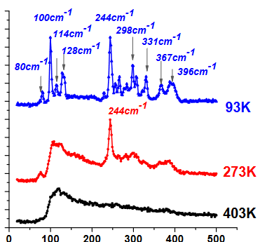
Luican-Mayer, Adina; Guest, Jeffrey R.; Hla, Saw-Wai
Suppression of charge density wave phases in ultrathin 1T-TaS2 Journal Article
In: Physical review letters, vol. 100 , no. 165414 , 2015.
@article{arXiv:1506.04102v1,

title = {Suppression of charge density wave phases in ultrathin 1T-TaS2},

author = {Adina Luican-Mayer and Jeffrey R. Guest and Saw-Wai Hla},

url = {https://arxiv.org/abs/1506.04102},

year  = {2015},

date = {2015-06-12},

urldate = {2015-06-12},

journal = {Physical review letters},

volume = {100 },

number = {165414 },

abstract = {Using temperature dependent Raman spectroscopy we address the question of how the transition from bulk to few atomic layers affects the charge density wave (CDW) phases in 1T-TaS2. We find that for crystals with thickness larger than approx 10nm the transition temperatures between the different phases as well as the hysteresis that occurs in the thermal cycle correspond to the ones expected for a bulk sample. However, when the crystals become thinner than ≈10nm, the commensurate CDW phase is suppressed down to the experimentally accessible temperatures. In addition, the nearly commensurate CDW phase is diminished below approx 4nm. These findings suggest that the interlayer coupling plays a significant role in determining the properties of CDW systems consisting of a few unit cells in the vertical direction. },

keywords = {},

pubstate = {published},

tppubtype = {article}

}
Lu, Chih-Pin; Rodriguez-Vega, Martin; Li, Guohong; Luican-Mayer, Adina; Watanabe, K.; Taniguchi, T.; Rossi, Enrico; Andrei, Eva Y.
Local and Global Screening Properties of Graphene Revealed through Landau Level Spectroscopy Journal Article
In: Proceedings of the National Academy of Sciences, vol. 113, no. 6623, 2015.
@article{arXiv:1504.07540v1,

title = {Local and Global Screening Properties of Graphene Revealed through Landau Level Spectroscopy},

author = {Chih-Pin Lu and Martin Rodriguez-Vega and Guohong Li and Adina Luican-Mayer and K. Watanabe and T. Taniguchi and Enrico Rossi and Eva Y. Andrei},

url = {https://arxiv.org/abs/1504.07540},

year  = {2015},

date = {2015-04-28},

urldate = {2015-04-28},

journal = {Proceedings of the National Academy of Sciences},

volume = {113},

number = {6623},

abstract = {One-atom thick crystalline layers and their vertical heterostructures carry the promise of designer electronic materials that are unattainable by standard growth techniques. In order to realize their potential it is necessary to isolate them from environmental disturbances in particular those introduced by the substrate. But finding and characterizing suitable substrates, and minimizing the random potential fluctuations they introduce, has been a persistent challenge in this emerging field. Here we show that Landau-level (LL) spectroscopy is exquisitely sensitive to potential fluctuations on both local and global length scales. Harnessing this technique we demonstrate that the insertion of an intermediate graphene layer provides superior screening of substrate induced disturbances, more than doubling the electronic mean free path. Furthermore, we find that the proximity of hBN acts as a nano-scale vacuum cleaner, dramatically suppressing the global potential fluctuations. This makes it possible to fabricate high quality devices on standard SiO2 substrates. },

keywords = {},

pubstate = {published},

tppubtype = {article}

}
Wang, YL; Thoutam, LR; Xiao, ZL; Hu, J; Das, S; Mao, ZQ; Wei, J; Divan, R; Luican-Mayer, A; Crabtree, GW; others,
Origin of the turn-on temperature behavior in WTe 2 Journal Article
In: Physical Review B, vol. 92, no. 18, pp. 180402, 2015.
@article{wang2015origin,

title = {Origin of the turn-on temperature behavior in WTe 2},

author = {YL Wang and LR Thoutam and ZL Xiao and J Hu and S Das and ZQ Mao and J Wei and R Divan and A Luican-Mayer and GW Crabtree and others},

url = {https://link.aps.org/doi/10.1103/PhysRevB.92.180402},

doi = {10.1103/PhysRevB.92.180402},

year  = {2015},

date = {2015-01-01},

urldate = {2015-01-01},

journal = {Physical Review B},

volume = {92},

number = {18},

pages = {180402},

publisher = {APS},

abstract = {A hallmark of materials with extremely large magnetoresistance (XMR) is the transformative turn-on temperature behavior: when the applied magnetic field H is above certain value, the resistivity versus temperature ρ(T) curve shows a minimum at a field dependent temperature T∗, which has been interpreted as a magnetic-field-driven metal-insulator transition or attributed to an electronic structure change. Here, we demonstrate that ρ(T) curves with turn-on behavior in the newly discovered XMR material WTe2 can be scaled as MR∼(H/ρ0)m with m≈2 and ρ0 being the resistivity at zero field. We obtained experimentally and also derived from the observed scaling the magnetic field dependence of the turn-on temperature T∗∼(H−Hc)ν with ν≈1/2, which was earlier used as evidence for a predicted metal-insulator transition. The scaling also leads to a simple quantitative expression for the resistivity ρ∗≈2ρ0 at the onset of the XMR behavior, which fits the data remarkably well. These results exclude the possible existence of a magnetic-field-driven metal-insulator transition or significant contribution of an electronic structure change to the low-temperature XMR in WTe2. This work resolves the origin of the turn-on behavior observed in several XMR materials and also provides a general route for a quantitative understanding of the temperature dependence of MR in both XMR and non-XMR materials.},

keywords = {},

pubstate = {published},

tppubtype = {article}

}
2014
Luican-Mayer, Adina; Kharitonov, Maxim; Li, Guohong; Lu, Chih-Pin; Skachko, Ivan; Gonçalves, Além-Mar B.; K. Watanabe, T. Taniguchi; and Eva Y. Andre,
Screening Charged Impurities and Lifting the Orbital Degeneracy in Graphene by Populating Landau Levels Journal Article
In: Phys. Rev. Lett., vol. 112, iss. 3, pp. 036804, 2014.
@article{PhysRevLett.112.036804,

title = {Screening Charged Impurities and Lifting the Orbital Degeneracy in Graphene by Populating Landau Levels},

author = {Adina Luican-Mayer and Maxim Kharitonov and Guohong Li and Chih-Pin Lu and Ivan Skachko and Além-Mar B. Gonçalves and K. Watanabe, T. Taniguchi and and Eva Y. Andre},

url = {https://link.aps.org/doi/10.1103/PhysRevLett.112.036804},

doi = {10.1103/PhysRevLett.112.036804},

year  = {2014},

date = {2014-01-01},

urldate = {2014-01-01},

journal = {Phys. Rev. Lett.},

volume = {112},

issue = {3},

pages = {036804},

publisher = {American Physical Society},

abstract = {We report the observation of an isolated charged impurity in graphene and present direct evidence of the close connection between the screening properties of a 2D electron system and the influence of the impurity on its electronic environment. Using scanning tunneling microscopy and Landau level spectroscopy, we demonstrate that in the presence of a magnetic field the strength of the impurity can be tuned by controlling the occupation of Landau-level states with a gate voltage. At low occupation the impurity is screened, becoming essentially invisible. Screening diminishes as states are filled until, for fully occupied Landau levels, the unscreened impurity significantly perturbs the spectrum in its vicinity. In this regime we report the first observation of Landau-level splitting into discrete states due to lifting the orbital degeneracy.},

keywords = {},

pubstate = {published},

tppubtype = {article}

}
2013
Li, Guohong; Luican-Mayer, Adina; Abanin, Dmitry; Levitov, Leonid; Andrei, Eva Y.
Evolution of Landau levels into edge states in graphene Journal Article
In: Nature communications, vol. 4, no. 1, pp. 1–7, 2013.
@article{li2013evolution,

title = {Evolution of Landau levels into edge states in graphene},

author = {Guohong Li and Adina Luican-Mayer and Dmitry Abanin and Leonid Levitov and Eva Y. Andrei},

url = {https://www.nature.com/articles/ncomms2767},

doi = {https://doi.org/10.1038/ncomms2767},

year  = {2013},

date = {2013-04-23},

urldate = {2013-01-01},

journal = {Nature communications},

volume = {4},

number = {1},

pages = {1--7},

publisher = {Nature Publishing Group},

abstract = {Two-dimensional electron systems in the presence of a magnetic field support topologically ordered states, in which the coexistence of an insulating bulk with conducting one-dimensional chiral edge states gives rise to the quantum Hall effect. For systems confined by sharp boundaries, theory predicts a unique edge-bulk correspondence, which is central to proposals of quantum Hall-based topological qubits. However, in conventional semiconductor-based two-dimensional electron systems, these elegant concepts are difficult to realize, because edge-state reconstruction due to soft boundaries destroys the edge-bulk correspondence. Here we use scanning tunnelling microscopy and spectroscopy to follow the spatial evolution of electronic (Landau) levels towards an edge of graphene supported above a graphite substrate. We observe no edge-state reconstruction, in agreement with calculations based on an atomically sharp boundary. Our results single out graphene as a system where the edge structure can be controlled and the edge-bulk correspondence is preserved.},

keywords = {},

pubstate = {published},

tppubtype = {article}

}
2012
Luican-Mayer, Adina
Scanning tunneling microscopy and spectroscopy studies of graphene PhD Thesis
2012.
@phdthesis{luican2012scanning,

title = {Scanning tunneling microscopy and spectroscopy studies of graphene},

author = {Adina Luican-Mayer},

url = {https://citeseerx.ist.psu.edu/viewdoc/download?doi=10.1.1.914.1608&rep=rep1&type=pdf},

year  = {2012},

date = {2012-01-01},

urldate = {2012-01-01},

publisher = {Citeseer},

abstract = {In the two-dimensional (2D) lattice of graphene, consisting of carbon atoms arranged in a honeycomb lattice, the charge carriers are described by a Dirac-Weyl Hamiltonian. Seeking to understand their unique nature, this thesis presents

results of scanning tunneling microscopy (STM) and spectroscopy (STS) experiments at low temperatures and in magnetic field. These techniques give access, down to atomic scales, to structural information as well as to the electronic properties of graphene.

The main findings include the observation of quantized Landau levels (LL) in the presence of magnetic field, their dependence on carrier density and effects of charged impurities and other disorder on the LL spectrum.

Twisting graphene layers away from the equilibrium Bernal stacking leads to the formation of Moiré patterns that significantly alter the electronic properties of graphene stacks. The second part of the thesis discusses the effects of such rotations on the electronic properties as a function of twist angle.},

keywords = {},

pubstate = {published},

tppubtype = {phdthesis}

}
results of scanning tunneling microscopy (STM) and spectroscopy (STS) experiments at low temperatures and in magnetic field. These techniques give access, down to atomic scales, to structural information as well as to the electronic properties of graphene.
The main findings include the observation of quantized Landau levels (LL) in the presence of magnetic field, their dependence on carrier density and effects of charged impurities and other disorder on the LL spectrum.
Twisting graphene layers away from the equilibrium Bernal stacking leads to the formation of Moiré patterns that significantly alter the electronic properties of graphene stacks. The second part of the thesis discusses the effects of such rotations on the electronic properties as a function of twist angle.
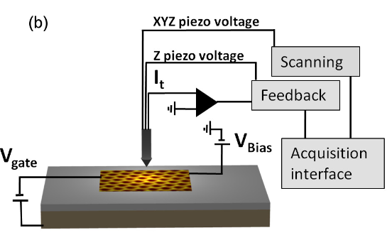
Luican-Mayer, Adina; Andrei, Eva Y.
Probing Dirac Fermions in Graphene by Scanning Tunneling Probes Journal Article
In: preprint, 2012.
@article{nokey,

title = {Probing Dirac Fermions in Graphene by Scanning Tunneling Probes},

author = {Adina Luican-Mayer and Eva Y. Andrei},

url = {https://citeseerx.ist.psu.edu/document?repid=rep1&type=pdf&doi=70beec360f28b661bccb784776bc1d1dd96b9b5b},

year  = {2012},

date = {2012-01-01},

urldate = {2012-01-01},

journal = {preprint},

abstract = {Graphene is a two dimensional system which can be studied using surface probe techniques such as scanning tunneling microscopy and spectroscopy. Combining the two, one can learn about the surface morphology as well as about its electronic properties. In this chapter we present a brief review of experimental results obtained on graphene supported on substrates with varying degrees of disorder. In the first part we focus on the electronic properties of single layer graphene without a magnetic field as well as in the presence of a perpendicular magnetic field. The second part focuses on twisted graphene stacks and the effects of rotating away from the equilibrium Bernal stacking on the electronic properties.},

keywords = {},

pubstate = {published},

tppubtype = {article}

}
2011
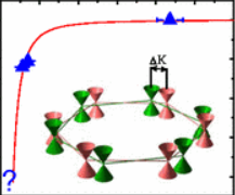
Luican, A.; Li, Guohong; Reina, A.; Kong, J.; Nair, R. R.; Novoselov, Konstantin S.; Geim, Andrei K.; Andrei, E. Y.
Single-layer behavior and its breakdown in twisted graphene layers Journal Article
In: Physical review letters, vol. 106, no. 12, pp. 126802, 2011.
@article{luican2011single,

title = {Single-layer behavior and its breakdown in twisted graphene layers},

author = {A. Luican and Guohong Li and A. Reina and J. Kong and R.R. Nair and Konstantin S. Novoselov and Andrei K. Geim and E.Y. Andrei},

url = {https://link.aps.org/doi/10.1103/PhysRevLett.106.126802},

doi = {10.1103/PhysRevLett.106.126802},

year  = {2011},

date = {2011-03-21},

urldate = {2011-01-01},

journal = {Physical review letters},

volume = {106},

number = {12},

pages = {126802},

publisher = {APS},

abstract = {We report high magnetic field scanning tunneling microscopy and Landau level spectroscopy of twisted graphene layers grown by chemical vapor deposition. For twist angles exceeding ∼3° the low energy carriers exhibit Landau level spectra characteristic of massless Dirac fermions. Above 20° the layers effectively decouple and the electronic properties are indistinguishable from those in single-layer graphene, while for smaller angles we observe a slowdown of the carrier velocity which is strongly angle dependent. At the smallest angles the spectra are dominated by twist-induced van Hove singularities and the Dirac fermions eventually become localized. An unexpected electron-hole asymmetry is observed which is substantially larger than the asymmetry in either single or untwisted bilayer graphene.},

keywords = {},

pubstate = {published},

tppubtype = {article}

}
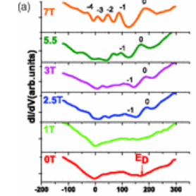
Luican, Adina; Li, Guohong; Andrei, Eva Y.
Quantized Landau level spectrum and its density dependence in graphene Journal Article
In: Physical Review B, vol. 83, no. 4, pp. 041405, 2011.
@article{luican2011quantized,

title = {Quantized Landau level spectrum and its density dependence in graphene},

author = {Adina Luican and Guohong Li and Eva Y. Andrei},

url = {https://link.aps.org/doi/10.1103/PhysRevB.83.041405},

doi = {10.1103/PhysRevB.83.041405},

year  = {2011},

date = {2011-01-27},

urldate = {2011-01-27},

journal = {Physical Review B},

volume = {83},

number = {4},

pages = {041405},

publisher = {APS},

abstract = {Scanning tunneling microscopy and spectroscopy in a magnetic field was used to study Landau quantization in graphene and its dependence on charge carrier density. Measurements were carried out on exfoliated graphene samples deposited on a chlorinated SiO2 thermal oxide, which allowed for the observation of the Landau level sequences characteristic of single-layer graphene while tuning the density through the Si backgate. Upon changing the carrier density, we find abrupt jumps in the Fermi level after each Landau level is filled. Moreover, at low doping levels, a marked increase in the Fermi velocity is observed, which is consistent with the logarithmic divergence expected due to the onset of many-body effects close to the Dirac point.},

keywords = {},

pubstate = {published},

tppubtype = {article}

}
Li, Guohong; Luican, Adina; Andrei, Eva Y
Self-navigation of a scanning tunneling microscope tip toward a micron-sized graphene sample Journal Article
In: Review of Scientific Instruments, vol. 82, no. 7, pp. 073701, 2011.
@article{li2011self,

title = {Self-navigation of a scanning tunneling microscope tip toward a micron-sized graphene sample},

author = {Guohong Li and Adina Luican and Eva Y Andrei},

url = {https://aip.scitation.org/doi/10.1063/1.3605664},

doi = {https://doi.org/10.1063/1.3605664},

year  = {2011},

date = {2011-01-01},

urldate = {2011-01-01},

journal = {Review of Scientific Instruments},

volume = {82},

number = {7},

pages = {073701},

publisher = {American Institute of Physics},

abstract = {We demonstrate a simple capacitance-based method to quickly and efficiently locate micron-sized conductive samples, such as graphene flakes, on insulating substrates in a scanning tunneling microscope (STM). By using edge recognition, the method is designed to locate and to identify small features when the STM tip is far above the surface, allowing for crash-free search and navigation. The method can be implemented in any STM environment, even at low temperatures and in strong magnetic field, with minimal or no hardware modifications.

},

keywords = {},

pubstate = {published},

tppubtype = {article}

}
2010
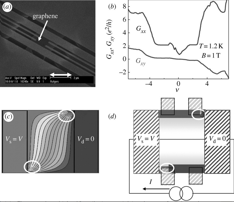
X. Du I. Skachko, F. Duerr; Andrei, E. Y.
Fractional quantum Hall effect in suspended graphene probed with two-terminal measurements Journal Article
In: Royal Society, vol. 368, iss. 1932, 2010.
@article{nokey,

title = {Fractional quantum Hall effect in suspended graphene probed with two-terminal measurements},

author = {I. Skachko, X. Du, F. Duerr, A. Luican-Mayer, D. A. Abanin, L. S. Levitov and E. Y. Andrei},

url = {https://royalsocietypublishing.org/doi/pdf/10.1098/rsta.2010.0226},

year  = {2010},

date = {2010-12-13},

journal = {Royal Society},

volume = {368},

issue = {1932},

abstract = {Recently, fractional quantization of two-terminal conductance was reported in suspended graphene. The quantization, which was clearly visible in fields as low as 2 T and persistent up to 20 K in 12 T, was attributed to the formation of an incompressible fractional quantum Hall state. Here, we argue that the failure of earlier experiments to detect the integer and fractional quantum Hall effect with a Hall-bar lead geometry is a consequence of the invasive character of voltage probes in mesoscopic samples, which are easily shorted out owing to the formation of hot spots near the edges of the sample. This conclusion is supported by a detailed comparison with a solvable transport model. We also consider, and rule out, an alternative interpretation of the quantization in terms of the formation of a p–n–p junction, which could result from contact doping or density inhomogeneity. Finally, we discuss the estimate of the quasi-particle gap of the quantum Hall state. The gap value, obtained from the transport data using a conformal mapping technique, is considerably larger than in GaAs-based two-dimensional electron systems, reflecting the stronger Coulomb interactions in graphene.},

keywords = {},

pubstate = {published},

tppubtype = {article}

}
2009
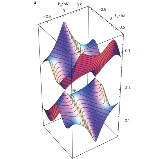
Li, Guohong; Luican, A; dos Santos, J M B Lopes; Neto, A H Castro; Reina, A; Kong, J; Andrei, E Y
Observation of Van Hove singularities in twisted graphene layers Journal Article
In: Nature Physics, vol. 6, no. 2, pp. 109–113, 2009, ISSN: 1745-2481.
@article{li_observation_2010,

title = {Observation of Van Hove singularities in twisted graphene layers},

author = {Guohong Li and A Luican and J M B Lopes dos Santos and A H Castro Neto and A Reina and J Kong and E Y Andrei},

url = {https://www.nature.com/articles/nphys1463},

doi = {10.1038/nphys1463},

issn = {1745-2481},

year  = {2009},

date = {2009-11-29},

urldate = {2010-01-01},

journal = {Nature Physics},

volume = {6},

number = {2},

pages = {109--113},

abstract = {Electronic instabilities at the crossing of the Fermi energy with a Van Hove singularity1 in the density of states often lead to new phases of matter such as superconductivity2,3, magnetism4 or density waves5. However, in most materials this condition is difficult to control. In the case of single-layer graphene, the singularity is too far from the Fermi energy6 and hence difficult to reach with standard doping and gating techniques7. Here we report the observation of low-energy Van Hove singularities in twisted graphene layers seen as two pronounced peaks in the density of states measured by scanning tunnelling spectroscopy. We demonstrate that a rotation between stacked graphene layers can generate Van Hove singularities, which can be brought arbitrarily close to the Fermi energy by varying the angle of rotation. This opens intriguing prospects for Van Hove singularity engineering of electronic phases.},

keywords = {},

pubstate = {published},

tppubtype = {article}

}
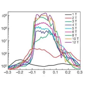
Du, Xu; Skachko, Ivan; Duerr, Fabian; Luican, Adina; Andrei, Eva Y
Fractional quantum Hall effect and insulating phase of Dirac electrons in graphene Journal Article
In: Nature, vol. 462, no. 7270, pp. 192-195, 2009, ISSN: 1476-4687.
@article{Du2009b,

title = {Fractional quantum Hall effect and insulating phase of Dirac electrons in graphene},

author = {Xu Du and Ivan Skachko and Fabian Duerr and Adina Luican and Eva Y Andrei},

url = {https://doi.org/10.1038/nature08522},

doi = {10.1038/nature08522},

issn = {1476-4687},

year  = {2009},

date = {2009-11-01},

urldate = {2009-11-01},

journal = {Nature},

volume = {462},

number = {7270},

pages = {192-195},

abstract = {The fractional quantum Hall effect is a quintessential manifestation of the collective behaviour associated with strongly interacting charge carriers confined to two dimensions and subject to a strong magnetic field. It is predicted that the charge carriers present in graphene --- an atomic layer of carbon that can be seen as the 'perfect' two-dimensional system --- are subject to strong interactions. Nevertheless, the phenomenon had eluded experimental observation until now: in this issue two groups report fractional quantum Hall effect in suspended sheets of graphene, probed in a two-terminal measurement setup. The researchers also observe a magnetic-field-induced insulating state at low carrier density, which competes with the quantum Hall effect and limits its observation to the highest-quality samples only. These results pave the way for the study of the rich collective behaviour of Dirac fermions in graphene.},

keywords = {},

pubstate = {published},

tppubtype = {article}

}
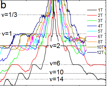
Skachko, I.; Du, X.; Duerr, F.; Luican, A.; Abanin, D. A.; Levitov, L. S.; Andrei, E. Y.
Integer and fractional quantum hall effect in two-terminal measurements on suspended graphene Journal Article
In: arXiv preprint arXiv:0910.2518, 2009.
@article{skachko2009integer,

title = {Integer and fractional quantum hall effect in two-terminal measurements on suspended graphene},

author = {I. Skachko and X. Du and F. Duerr and A. Luican and D.A. Abanin and L.S. Levitov and E.Y. Andrei},

url = {https://arxiv.org/abs/0910.2518},

doi = {10.1098/rsta.2010.0226},

year  = {2009},

date = {2009-10-14},

urldate = {2009-01-01},

journal = {arXiv preprint arXiv:0910.2518},

abstract = {We report the observation of the quantized Hall effect in suspended graphene probed with a two-terminal lead geometry. The failure of earlier Hall-bar measurements is discussed and attributed to the placement of voltage probes in mesoscopic samples. New quantized states are found at integer Landau level fillings outside the sequence 2,6,10.., as well as at a fractional filling nu=1/3. Their presence is revealed by plateaus in the two-terminal conductance which appear in magnetic fields as low as 2 Tesla at low temperatures and persist up to 20 Kelvin in 12 Tesla. The excitation gaps, extracted from the data with the help of a theoretical model, are found to be significantly larger than in GaAs based electron systems.},

keywords = {},

pubstate = {published},

tppubtype = {article}

}
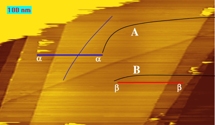
Luican-Mayer, Adina; Li, Guohong; Andrei, Eva Y.
Scanning tunneling spectroscopy of graphene on graphite Journal Article
In: Physical review letters, vol. 102, iss. 17, pp. 176804, 2009.
@article{nokey,

title = {Scanning tunneling spectroscopy of graphene on graphite},

author = {Adina Luican-Mayer and Guohong Li and Eva Y. Andrei},

url = {https://journals.aps.org/prl/pdf/10.1103/PhysRevLett.102.176804},

year  = {2009},

date = {2009-05-01},

urldate = {2009-05-01},

journal = {Physical review letters},

volume = {102},

issue = {17},

pages = {176804},

abstract = {We report low temperature high magnetic field scanning tunneling microscopy and spectroscopy of graphene flakes on graphite that exhibit the structural and electronic properties of graphene decoupled from the substrate. Pronounced peaks in the tunneling spectra develop with increasing field revealing a Landau level sequence that provides a direct way to identify graphene and to determine the degree of its coupling to the substrate. The Fermi velocity and quasiparticle lifetime, obtained from the positions and width of the peaks, provide access to the electron-phonon and electron-electron interactions.},

keywords = {},

pubstate = {published},

tppubtype = {article}

}
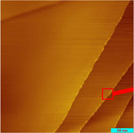
Luican, Adina; Li, Guohong; Andrei, Eva Y.
Scanning tunneling microscopy and spectroscopy of graphene layers on graphite Journal Article
In: Solid State Communications, vol. 149, no. 27-28, pp. 1151–1156, 2009.
@article{luican2009scanning,

title = {Scanning tunneling microscopy and spectroscopy of graphene layers on graphite},

author = {Adina Luican and Guohong Li and Eva Y. Andrei},

url = {https://www.sciencedirect.com/science/article/abs/pii/S0038109809001446},

doi = {https://doi.org/10.1016/j.ssc.2009.02.059},

year  = {2009},

date = {2009-03-29},

urldate = {2009-01-01},

journal = {Solid State Communications},

volume = {149},

number = {27-28},

pages = {1151--1156},

publisher = {Elsevier},

abstract = {We report low temperature scanning tunneling microscopy and spectroscopy on graphene flakes supported on a graphite substrate. The experiments demonstrate that graphite is exceptionally well suited as a substrate for graphene because it offers support without disturbing the intrinsic properties of the charge carriers. The degree of coupling of a graphene flake to the substrate was recognized and characterized from the appearance of an anomalous Landau level sequence in the presence of a perpendicular magnetic field. By following the evolution of the Landau level spectra along the surface, we identified graphene flakes that are decoupled or very weakly coupled to the substrate. From the Landau level sequence in this flake, we extract the local Fermi velocity and energy of the Dirac point and find extremely weak spatial variation of these quantities confirming the high quality and non invasive nature of the graphite substrate.},

keywords = {},

pubstate = {published},

tppubtype = {article}

}
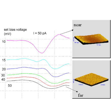
Li, Guohong; Luican, Adina; Andrei, Eva Y.
Electronic states on the surface of graphite Journal Article
In: Physica B: Condensed Matter, vol. 404, no. 18, pp. 2673–2677, 2009.
@article{li2009electronic,

title = {Electronic states on the surface of graphite},

author = {Guohong Li and Adina Luican and Eva Y. Andrei},

url = {https://www.sciencedirect.com/science/article/abs/pii/S0921452609004165},

doi = {https://doi.org/10.1016/j.physb.2009.06.071},

year  = {2009},

date = {2009-01-01},

urldate = {2009-01-01},

journal = {Physica B: Condensed Matter},

volume = {404},

number = {18},

pages = {2673--2677},

publisher = {Elsevier},

abstract = {Graphite consists of graphene layers in an AB (Bernal) stacking arrangement. The introduction of defects can reduce the coupling between the top graphene layers and the bulk crystal producing new electronic states that reflect the degree of coupling. We employ low temperature high magnetic field scanning tunneling microscopy (STM) and spectroscopy (STS) to access these states and study their evolution with the degree of coupling. STS in magnetic field directly probes the dimensionality of electronic states. Thus two-dimensional states produce a discrete series of Landau levels while three-dimensional states form Landau bands providing a clear distinction between completely decoupled top layers and ones that are coupled to the substrate. We show that the completely decoupled layers are characterized by a single sequence of Landau levels with square-root dependence on field and level index indicative of massless Dirac fermions. In contrast weakly coupled bilayers produce special sequences reflecting the degree of coupling, and multilayers produce sequences reflecting the coexistence of massless and massive Dirac fermions. In addition we show that the graphite surface is soft and that an STM tip can be quite invasive when brought too close to the surface and that there is a characteristic tip–sample distance beyond which the effect of sample–tip interaction is negligible.},

keywords = {},

pubstate = {published},

tppubtype = {article}

}